Hot Keywords:
- All
- Product Name
- Product Keyword
- Product Model
- Product Summary
- Product Description
- Multi Field Search
Views: 0 Author: Site Editor Publish Time: 2025-05-07 Origin: Site
We talked recently about ion implantation, for example:
Why ion implantation?
Why do you have to deviate from a certain Angle when you inject ions?
However, the implementation of this technology inevitably causes damage to the crystal structure of silicon wafers. This damage originates from atomic-level collisions triggered by high-energy ions penetrating the silicon lattice. When high-energy ions bombard silicon materials, their enormous kinetic energy disrupts the original atomic arrangement, leading to lattice distortion, vacancy formation, and the accumulation of interstitial atoms.
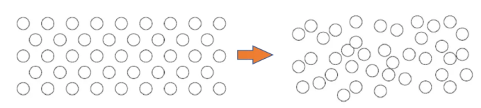
Before After
These micro defects will not only form the composite center to reduce the carrier mobility, but also may cause the local band structure distortion, which will seriously affect the electrical performance of the device.
In order to eliminate the negative effects of ion implantation, thermal annealing is a key step in repairing lattice damage. By placing silicon wafers with implanted impurities in a specific temperature environment for thermal treatment, lattice atoms can be rearranged and restored to an ordered structure.
In this process, impurity atoms migrate from the initial gap position to the lattice substitution site, so as to restore the integrity of the lattice and realize the electrical activation of impurities.
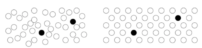
Before After
Conventional thermal annealing is usually carried out in the temperature range of 600-1000℃. The high temperature environment provides sufficient energy for atomic diffusion, but long time heat treatment may lead to excessive diffusion of impurities and change the pre-designed doping distribution profile.
This disadvantage is particularly prominent in the fine nano-scale process, where the thermal diffusion of impurities can easily break through the design size limit and cause deviation of transistor performance.
In order to break through the limitations of traditional annealing process, rapid annealing technology (RTA) has emerged. This technology uses high energy density heat source to achieve rapid heating and short time treatment, including pulse laser annealing, electron beam annealing and xenon lamp flash annealing.